


JOIN

LOGIN
 Custom Made Order
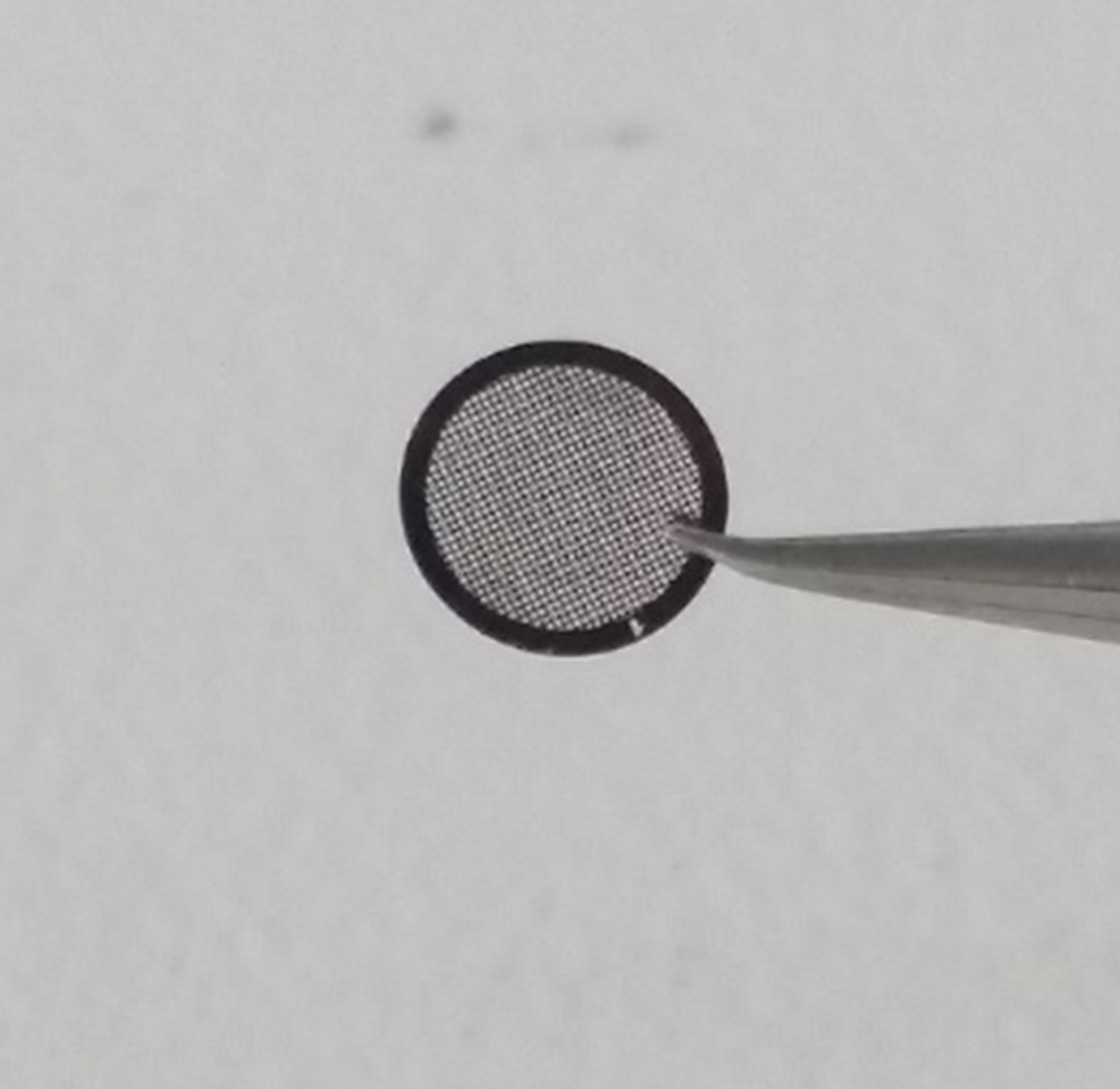
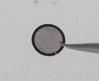
We provide transfer services of TCVD Grown Monolayer Graphene on Cu on top of TEM Grid in order for you to be able to make measurement of Transmission Electron Microscope
Properties
| TEM Grid Graphene | ||
|---|---|---|
| Grid Hole Size : 63خ¼m | Sheet Resistance : Av.< 250~400 خ©/sq | |
| Lacey Carbon Type-A | Mobility : >3500مژ /Vs (Max. 17,000 مژ /Vs | |
| 300 mesh | Transmittance : >97% | |
| Copper Frame | Coverage : <30% (PMMA-free), <60% (2-layers) | |
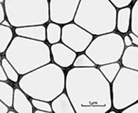
Lacey Carbon Type-A
A Lacey carbon film with a removable Formvar backing on the opposite side of the grid. When the Formvar is removed, by dipping in solvent, the Lacey carbon film remains. These films are stable under all EM(electron microscopy) operating conditions and for use where the presence of Formvar can not be tolerated. Pure Lacey Carbon is more delicate than those with Formvar backing and require more careful handling during specimen preparation. Holes are completely open.
Lacey Support Film
Bare TEM Grid
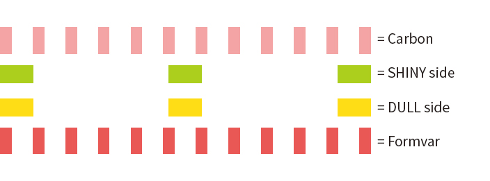
Support Film Product Note, How the Material is Layered on the Grid
Most of the grids used have a distinct “shiny†side and “dull†side when viewed with the naked eye. Generally, the film type as specified in the product name lies on the shiny side of the grid.
Lacey carbon Type A
The Lacey formvar film is applied to the dull side of the grid and carbon depositied onto the shiny side. When the formvar is removed in solvent the carbon film is left on the shiny side.
Grid Cross Section
| Substrate Application | Carbon Type-A | Is Lacey Film suitable for this application? |
|---|---|---|
| Applications Requiring Pure Formvar | Not Suitable | No |
| Bacterial Suspensions | Best | Yes |
| Cell Fragment Suspensions | Best | Yes |
| Diffraction Studies | Best | Yes |
| EDS (energy dispersive spectrometry) | Best | Yes |
| High Resolution Microscopy | Best | Yes |
| High Temperature Techniques / Heating Stage | Best | Yes(Type-A) |
| Low Magnification Microscopy | Good Alternative | No |
| Particulate Suspension, Biological | Best | Yes |
| Particulate Suspension, Non-Biological | Best | Yes |
| Powders, Dry | Good Alternative | No |
| Replicas & Low Temperature Techniques | Good Alternative | Yes(Type-A) |
| Thin Sections | Good Alternative | Yes |
| Viral Suspensions | Best | Yes |
Measurement data
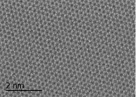
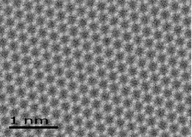
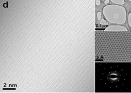
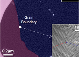
(d) HR-TEM results showing the atomic lattice structures of RT-CVD graphene. The graphene samples were prepared with holey carbon grid (upper inset). The aberration-corrected scanning TEM image provides an atom-by-atom analysis of graphene (mid inset). The diffraction pattern indicates the corresponding graphene is a highly crystalline monolayer (lower inset). (e) Graphene domain distribution investigated by selected area diffraction patterns (SADP) and TEM imaging. (f) Graphene boundaries of RT-CVD graphene characterized by dark-field TEM and aberration-corrected HR-TEM images . The left and right parts of the grain boundary are imaged with an aperture at the red and blue circled spots of the diffraction pattern (upper inset). The atomic image shows that two graphene domains are smoothly connected with an angle of 36آ° (lower inset). See also Supporting Figure S2 for more dark-field TEM analyses.
Spot 1 (top)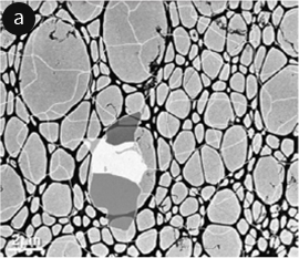
Spot 2 (center)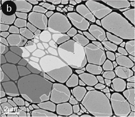
Spot 3 (bottom)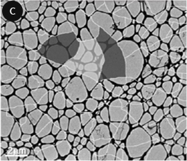
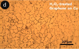
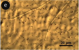
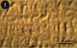
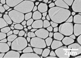
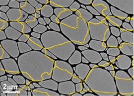
Figure 4. Grain boundary analyses by TEM and OM. (a-c) Grain boundary mapping of RT-CVD graphene films by TEM corresponding to the sheet resistance of spots 1, 2, and 3 in Figure 3a, respectively. (d-f) Grain boundary mapping of H2O2-treated RT-CVD graphene on Cu foils by optical microscopes, corresponding to the red spots 1, 2, and 3 in Figure 3a, respectively. The grain size of graphene in the center region is a few times larger than the edge region. But actually, there is no significant difference in sheet resistance (226, 227, and 230 Ω/sq for spots 1, 2, and 3, respectively).
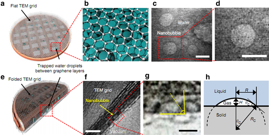
Figure 1 | Morphology of nanobubbles in graphene liquid cell. (a?d) A graphene liquid cell fabricated on a ?at TEM grid (copper or molybdenum) showing the top views of nanobubbles. (c and d) In-situ snapshot images of nanobubbles obtained by ultra-high vacuum (UHV) TEM (200 keV, ~5X10⁻⁹ Torr). Scale bars, 10 nm. (e?g) A folded graphene liquid cell showing the side views of nanobubbles. The contact angles were roughly measured to be 6oآ°?90آ°. Scale bars for f and g, 10 and 5 nm, respectively.
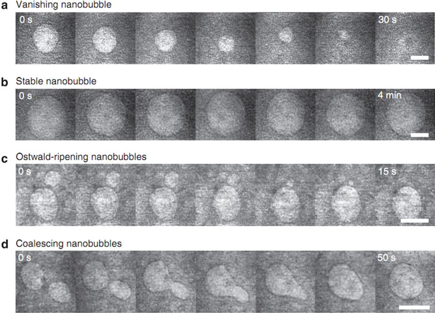
Figure 2 l Time evolution of different kinds of single and double nanobubbles. (a,b) The snap shots of Tem images showing the vanishing and stable nanobubbles, respectively. The nanobubbles smaller than critical radius tend to shrink with time and disappear in ~40s, whereas the larger bubbles persist for more than 10 min. Scale bar, 5 nm. The full movie is available in Supplementary Movie 2. (c,d) The snap shots of TEM images showing the merging of adjacent two nanobubbles observed for 15 and 50 s, respectively. When the nanobubble sizes are significantly different, it show an Ostwald ripening-like merging process, whereas the similar-sized bubbles are coalescing as their inter-bubble boundary breaks. Scale bar, 10nm. The full movie is available in Supplementary Movie 3.
Reference
(1) Ryu, Jaechul, et al. "Fast synthesis of high-performance graphene films by hydrogen-free rapid thermal chemical vapor deposition.†ACS nano 8.1 (2014): 950-956.
(2) Park, Jooyeon, et al. “Graphene‒Regulated Cardiomyogenic Differentiation Process of Mesenchymal Stem Cells by Enhancing the Expression of Extracellular Matrix Proteins and Cell Signaling Molecules.†Advanced healthcare materials 3.2 (2014): 176-181.
(3) Shin, Dongha, et al. “Growth dynamics and gas transport mechanism of nanobubbles in graphene liquid cells." Nature communications 6 (2015).
(4) Kim, Yeonho, et al. "High-performance ultraviolet photodetectors based on solution-grown ZnS nanobelts sandwiched between graphene layers." Scientific reports 5 (2015).
(5) Sim, Uk, et al. "N-doped graphene quantum sheets on silicon nanowire photocathodes for hydrogen production." Energy & Environmental Science 8.4 (2015): 1329-1338.
(6) Moon, Joonhee, et al. "Oneâ€گStep Synthesis of Nâ€گdoped Graphene Quantum Sheets from Monolayer Graphene by Nitrogen Plasma." Advanced Materials 26.21 (2014): 3501-3505.
(7) Kim, Sang Jin, et al. "Simultaneous etching and doping by Cu-stabilizing agent for high-performance graphene-based transparent electrodes." Chemistry of Materials 26.7 (2014): 2332-2336.
(8) Kim, Jung Kyu, et al. "Surface-Engineered Graphene Quantum Dots Incorporated into Polymer Layers for High Performance Organic Photovoltaics." Scientific reports 5 (2015).
-
Graphene Square Advantages
-
World’s first large scale graphene synthesis towards commercialization.
Nature Nanotechnology 2010 cover image.
-
Many years of know-how in transfer method.
Coverage at above 95%, low residue. Most optimized R&D environment.
-
Our sample package is designed to minimize graphene damage.
Vacuum packaged, nitrogen filled. Easy to handle.
-
Optimized Graphene
We give advice and make suggestions to the beginners in graphene research. Offer Graphene on various and unique substrates.
-
Our commitment
We promise to deliver a level of quality unmatched and to our customers’ satisfaction.
-
All about Graphene-from thermal CVD equipment to graphene synthesis and transfer process with know-how.
Understanding of the whole process from the graphene synthesis, transfer, proper packaging with sound research is our key to success.
-
-
Delivery Packaging Process
- 01 Vacuum packaging, nitrogen filled
-
 02
Air cushion packaging
02
Air cushion packaging
-
03
Ready for pick up by
courier service
Order processOrder process  Customer order and payment confirmation
 Produce graphene
 Packaging
 Delivery
Status Review and confirm customer order Produce and inspect for high quality product Expert and protective packaging for S&H Estimated time of delivery is three business days Detailed shipment tracking on fedex.com -
FAQ
-
I would like to know Graphene Square’s graphene synthesis and transfer process.
1) Graphene synthesis process by Thermal CVD equipment
2) PMMA coating
3) Back side etching (using RIE)
4) Cu foil etching using APS solution
5) Rinse using DIW water
6) Transfer onto substrate, dry by baking on hot plate
7) Remove PMMA by dipping in Acetone
8) Quality check (Optical microscope, Raman spectroscope)
9) Vacuum package, shipping -
Are you able to offer CVD Graphene on Cu foil in sizes besides what is currently being offered?
Currently, the smallest size we offer [TCVD Graphene on Cu foil] is 50x50mm while the larger size offered is 80x80mm. If you are in need of smaller sizes then what we offer, we suggest that you purchase a 50x50mm and cut into required sizes. If you need sizes larger then 80x80mm, then you can send and email to below email address. info@graphenesq.com
-
I am handling graphene for the first time and I am trying to start with graphene on substrates (SiO2/Si wafer, glass, PET,,,). Please advise.
It may be possible to purchase graphene on Cu foil and do the transfer process even as a beginner, however, there may be multiple trial and error processes. As a result, we would suggest purchasing our graphene transferred on substrates or if you are in need of our graphene transfer service, we can provide such service customers’ substrate as well. < Custom Made Order link >
-
For Stacked graphene, is the transfer process done after PMMA coating of each layer? If not, what is the transfer process for Stacked graphene?
For multiple layers, we use graphene on Cu foil to initiate and perform overlapping process. The basic process is as follows: take [Graphene/Cu foil] and scoop from underneath [PMMA/Graphene] using DI water bath resulting in [PMMA/Graphene/Graphene/Cu foil]. Afterwards, Cu foil can be etched away and the above process can be repeated to make multiple layers of graphene.
-
Can graphene be mixed and used to make products using product molds or presses?
As you may know, graphene can be acquired in two methods. 1) Top down: mechanically exfoliating carbon from graphite to make graphene powder or graphene oxide, 2) Bottom up: since carbon is composed of gas (ex. CH4, C2H4,,,) graphene film can be synthesized at high temperature through the CVD method. One of the options can be considered depending on the research goals. Due to graphene’s characteristics, the theoretical prices and actual sample prices can vary and the characteristics of graphene powder and graphene film differ as well. As a result, when mixing graphene with other materials, graphene powder may be more appropriate. You would have to perform tests to find the right mixture ratios, but generally, mixing graphene powder with other materials to further manufacture products using molds or presses are possible.
-
How can I make graphene samples on substrates using dry transfer method?
For dry transfer, there are two main options: 1) Thermal release tape [TRT], 2) Pressure Sensitive Adhesive Film [PSAF]. The common requirement is that both methods require pressure using a laminator.
1) TRT: apply TRT with level pressure and temperature (100~110℃) simultaneously so that graphene can be released from the base surface of TRT onto the target substrate [based upon long period of experience and know-how, TRT is the suggested option versus PSAF].
2) PSAF: apply PSAF with level pressure from the base surface of PSAF onto the target substrate.
-
I would like to know Graphene Square’s graphene synthesis and transfer process.
1) Graphene synthesis process by Thermal CVD equipment
2) PMMA coating
3) Back side etching (using RIE)
4) Cu foil etching using APS solution
5) Rinse using DIW water
6) Transfer onto substrate, dry by baking on hot plate
7) Remove PMMA by dipping in Acetone
8) Quality check (Optical microscope, Raman spectroscope)
9) Vacuum package, shipping
-
Are you able to offer CVD Graphene on Cu foil in sizes besides what is currently being offered?
Currently, the smallest size we offer [TCVD Graphene on Cu foil] is 50x50mm while the larger size offered is 80x80mm. If you are in need of smaller sizes then what we offer, we suggest that you purchase a 50x50mm and cut into required sizes. If you need sizes larger then 80x80mm, then you can send an email request to below email address. info@graphenesq.com
-
I would like to know Graphene Square’s graphene synthesis and transfer process.
1) Graphene synthesis process by Thermal CVD equipment
2) PMMA coating
3) Back side etching (using RIE)
4) Cu foil etching using APS solution
5) Rinse using DIW water
6) Transfer onto substrate, dry by baking on hot plate
7) Remove PMMA by dipping in Acetone
8) Quality check (Optical microscope, Raman spectroscope)
9) Vacuum package, shipping
-
I am handling graphene for the first time and I am trying to start with graphene on substrates (SiO2/Si wafer, glass, PET,,,). Please advise.
It may be possible to purchase graphene on Cu foil and do the transfer process even as a beginner, however, there may be multiple trial and error processes. As a result, we would suggest purchasing our graphene transferred on substrates or if you are in need of our graphene transfer service, we provide such service on customers' substrates as well. < Custom Made Order link >
-
I would like to know Graphene Square’s graphene synthesis and transfer process.
1) Graphene synthesis process by Thermal CVD equipment
2) PMMA coating
3) Back side etching (using RIE)
4) Cu foil etching using APS solution
5) Rinse using DIW water
6) Transfer onto substrate, dry by baking on hot plate
7) Remove PMMA by dipping in Acetone
8) Quality check (Optical microscope, Raman spectroscope)
9) Vacuum package, shipping
-
Can graphene be mixed and used to make products using product molds or presses?
As you may know, graphene can be acquired in two methods. 1) Top down: mechanically exfoliating carbon from graphite to make graphene powder or graphene oxide, 2) Bottom up: since carbon is composed of gas (ex. CH4, C2H4,,,) graphene film can be synthesized at high temperature through the CVD method. One of the options can be considered depending on the research goals. Due to graphene’s characteristics, the theoretical prices and actual sample prices can vary and the characteristics of graphene powder and graphene film differ as well. As a result, when mixing graphene with other materials, graphene powder may be more appropriate. You would have to perform tests to find the right mixture ratios, but generally, mixing graphene powder with other materials to further manufacture products using molds or presses are possible.
-
I would like to know Graphene Square’s graphene synthesis and transfer process.
1) Graphene synthesis process by Thermal CVD equipment
2) PMMA coating
3) Back side etching (using RIE)
4) Cu foil etching using APS solution
5) Rinse using DIW water
6) Transfer onto substrate, dry by baking on hot plate
7) Remove PMMA by dipping in Acetone
8) Quality check (Optical microscope, Raman spectroscope)
9) Vacuum package, shipping -
How can I make graphene samples on substrates using dry transfer method?
For dry transfer, there are two main options: 1) Thermal Release Tape [TRT], 2) Pressure Sensitive Adhesive Film [PSAF]. The common requirement is that both methods require pressure using a laminator.
1) TRT: apply TRT with level pressure and temperature (100~110℃) simultaneously so that graphene can be released from the base surface of TRT onto the target substrate [based upon long period of experience and know-how, TRT is the suggested option versus PSAF].
2) PSAF: apply PSAF with level pressure from the base surface of PSAF onto the target substrate.
-
For Stacked graphene, is the transfer process done after PMMA coating of each layer? If not, what is the transfer process for Stacked graphene?
For multiple layers, we use graphene on Cu foil to initiate and perform overlapping process. The basic process is as follows: take [Graphene/Cu foil] and scoop from underneath [PMMA/Graphene] using DI water bath resulting in [PMMA/Graphene/Graphene/Cu foil]. Afterwards, Cu foil can etched away and the above process can be repeated to make multiple layers of graphene.
-