


JOIN

LOGIN
 Custom Made Order
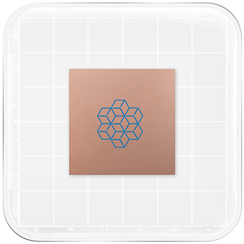
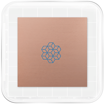

*Custom Size up to 1 x 1 m2 Available
Product and Service Overview
The state of the art chemical vapor deposition (CVD) method is used to synthesize our high-quality graphene products. It boasts more than 90% coverage of mono-layer graphene.
We also provide various studies and measurements on graphene samples to meet your need for high-end research and application.
- Properties of Graphene Film
- гҶҚProduct Size : Up to 500x600 гҺҹ
- гҶҚFilm morphology : Continuous Monolayer(>95%)
- гҶҚSheet Resistance : Av. < 250~400 О©/sq (after transfer)
- гҶҚMobility : >3500 гҺ /Vs
- гҶҚTransmittance : >97%
- гҶҚDomain Size : ~10гҺӣ
- Properties of Substrate
- гҶҚMaterial : Copper
- гҶҚPurity : ~99.9%
- гҶҚType : flexible foil
- гҶҚThickness : ~35гҺӣ
- Applications
- гҶҚTransparent electrode (flexible display & touch screen)
- гҶҚEnergy electrode (solar cells, secondary batteries, fuel cells, supercapacitors)
- гҶҚFunctional composite materials (ultra-light strong composite for cars & aerospace)
- гҶҚHeat dissipation (LED lighting & ECU units)
- гҶҚBarrier (gas barriers, electromagnetic wave barriers)
- гҶҚBiomedical applications (substrate for stem cell therapy, graphene liquid cells for electron microscopy)
- Main Target
Those who want to proceed directly to a Graphene transfer process
Measurement Data
Our CVD grown graphene is uniformly distributed with excellent coverage* Raman spectroscope measurement conditions
- Laser : 514 nm / Laser Power : 100% / Exposure time : 10s / Accumulation number : 1 / Hole size : 1um / Grating : 1200
-
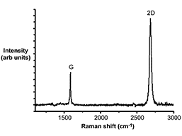
Raman Spectrum (after transfer)
-
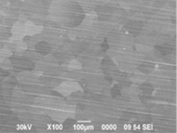
High Revolution SEM Image
-
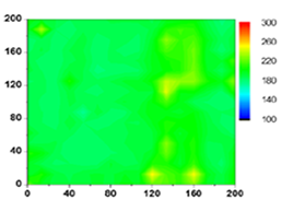
Sheet Resistance Uniformity
-
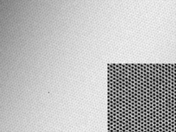
High Revolution TEM Image
- 1
S. Bae*, H. Kim* et al.Roll-to-roll production of 30 inch graphene films for transparent electrodes Nature Nanotech.5, 574 (2010).
- 2
Y. Lee et al. Wafer-Scale Synthesis and Transfer of Graphene Films. Nano Lett. 10, 490-493 (2010).
- 3
H.-A-S. Shin et al. Graphene-induced Unusual Microstructural Evolution in Ag Plated Cu Foils. Nanoscale 6, 7209-7214 (2014).
- 4
Hae-A-Seul Shin*, Jaychul Ryu* et al. Highly Uniform Growth of Monolayer Graphene by Chemical Vapor Deposition on Cu-Ag Alloy Catalysts. Phys. Chem. Chem. Phys. 16, 3087-3094 (2014).
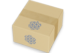
Packaging Process
 |
 |
 |
|
 |
|
 |
|---|---|---|---|---|---|---|
|
01protective packaging |
02Vacuum packaging, |
03Aircushion packaging |
04Ready for pick up by |
Customer List
| ETH Zurich | University of Exeter |
| Nokia Research Center | Sabanci University |
| Seoul National University | Korea Atomic Energy Research Institute |
| Intel Corporation | University of Oxford |
| Edicogenome | Korea Advanced Institute of Science and Technology |
| Ulsan National Institute of Science and Technology | Korea Basic Science Institute |
| University of Applied Sciences, Berlin | University of Westminster |
| Korea Institute of Science and Technology | Korea Institute of Ceramic |
| Korea University | Korea Aerospace University |
-
Graphene Square Advantages
-
WorldвҖҷs first large scale graphene synthesis towards commercialization.
Nature Nanotechnology 2010 cover image.
-
Many years of know-how in transfer method.
Coverage at above 95%, low residue. Most optimized R&D environment.
-
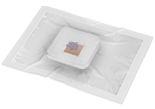
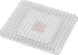
Our sample package is designed to minimize graphene damage.
Vacuum packaged, nitrogen filled. Easy to handle.
-
Optimized Graphene
We give advice and make suggestions to the beginners in graphene research. Offer Graphene on various and unique substrates.
-
Our commitment
We promise to deliver a level of quality unmatched and to our customersвҖҷ satisfaction.
-
All about Graphene-from thermal CVD equipment to graphene synthesis and transfer process with know-how.
Understanding of the whole process from the graphene synthesis, transfer, proper packaging with sound research is our key to success.
-
-
Delivery Packaging Process
- 01 Vacuum packaging, nitrogen filled
-
 02
Air cushion packaging
02
Air cushion packaging
-
03
Ready for pick up by
courier service
Order processOrder process  Customer order and payment confirmation
 Produce graphene
 Packaging
 Delivery
Status Review and confirm customer order Produce and inspect for high quality product Expert and protective packaging for S&H Estimated time of delivery is three business days Detailed shipment tracking on fedex.com -
FAQ
-
I would like to know Graphene SquareвҖҷs graphene synthesis and transfer process.
1) Graphene synthesis process by Thermal CVD equipment
2) PMMA coating
3) Back side etching (using RIE)
4) Cu foil etching using APS solution
5) Rinse using DIW water
6) Transfer onto substrate, dry by baking on hot plate
7) Remove PMMA by dipping in Acetone
8) Quality check (Optical microscope, Raman spectroscope)
9) Vacuum package, shipping -
Are you able to offer CVD Graphene on Cu foil in sizes besides what is currently being offered?
Currently, the smallest size we offer [TCVD Graphene on Cu foil] is 50x50mm while the larger size offered is 80x80mm. If you are in need of smaller sizes then what we offer, we suggest that you purchase a 50x50mm and cut into required sizes. If you need sizes larger then 80x80mm, then you can send and email to below email address. info@graphenesq.com
-
I am handling graphene for the first time and I am trying to start with graphene on substrates (SiO2/Si wafer, glass, PET,,,). Please advise.
It may be possible to purchase graphene on Cu foil and do the transfer process even as a beginner, however, there may be multiple trial and error processes. As a result, we would suggest purchasing our graphene transferred on substrates or if you are in need of our graphene transfer service, we can provide such service customersвҖҷ substrate as well. < Custom Made Order link >
-
For Stacked graphene, is the transfer process done after PMMA coating of each layer? If not, what is the transfer process for Stacked graphene?
For multiple layers, we use graphene on Cu foil to initiate and perform overlapping process. The basic process is as follows: take [Graphene/Cu foil] and scoop from underneath [PMMA/Graphene] using DI water bath resulting in [PMMA/Graphene/Graphene/Cu foil]. Afterwards, Cu foil can be etched away and the above process can be repeated to make multiple layers of graphene.
-
Can graphene be mixed and used to make products using product molds or presses?
As you may know, graphene can be acquired in two methods. 1) Top down: mechanically exfoliating carbon from graphite to make graphene powder or graphene oxide, 2) Bottom up: since carbon is composed of gas (ex. CH4, C2H4,,,) graphene film can be synthesized at high temperature through the CVD method. One of the options can be considered depending on the research goals. Due to grapheneвҖҷs characteristics, the theoretical prices and actual sample prices can vary and the characteristics of graphene powder and graphene film differ as well. As a result, when mixing graphene with other materials, graphene powder may be more appropriate. You would have to perform tests to find the right mixture ratios, but generally, mixing graphene powder with other materials to further manufacture products using molds or presses are possible.
-
How can I make graphene samples on substrates using dry transfer method?
For dry transfer, there are two main options: 1) Thermal release tape [TRT], 2) Pressure Sensitive Adhesive Film [PSAF]. The common requirement is that both methods require pressure using a laminator.
1) TRT: apply TRT with level pressure and temperature (100~110в„ғ) simultaneously so that graphene can be released from the base surface of TRT onto the target substrate [based upon long period of experience and know-how, TRT is the suggested option versus PSAF].
2) PSAF: apply PSAF with level pressure from the base surface of PSAF onto the target substrate.
-
I would like to know Graphene SquareвҖҷs graphene synthesis and transfer process.
1) Graphene synthesis process by Thermal CVD equipment
2) PMMA coating
3) Back side etching (using RIE)
4) Cu foil etching using APS solution
5) Rinse using DIW water
6) Transfer onto substrate, dry by baking on hot plate
7) Remove PMMA by dipping in Acetone
8) Quality check (Optical microscope, Raman spectroscope)
9) Vacuum package, shipping
-
Are you able to offer CVD Graphene on Cu foil in sizes besides what is currently being offered?
Currently, the smallest size we offer [TCVD Graphene on Cu foil] is 50x50mm while the larger size offered is 80x80mm. If you are in need of smaller sizes then what we offer, we suggest that you purchase a 50x50mm and cut into required sizes. If you need sizes larger then 80x80mm, then you can send an email request to below email address. info@graphenesq.com
-
I would like to know Graphene SquareвҖҷs graphene synthesis and transfer process.
1) Graphene synthesis process by Thermal CVD equipment
2) PMMA coating
3) Back side etching (using RIE)
4) Cu foil etching using APS solution
5) Rinse using DIW water
6) Transfer onto substrate, dry by baking on hot plate
7) Remove PMMA by dipping in Acetone
8) Quality check (Optical microscope, Raman spectroscope)
9) Vacuum package, shipping
-
I am handling graphene for the first time and I am trying to start with graphene on substrates (SiO2/Si wafer, glass, PET,,,). Please advise.
It may be possible to purchase graphene on Cu foil and do the transfer process even as a beginner, however, there may be multiple trial and error processes. As a result, we would suggest purchasing our graphene transferred on substrates or if you are in need of our graphene transfer service, we provide such service on customers' substrates as well. < Custom Made Order link >
-
I would like to know Graphene SquareвҖҷs graphene synthesis and transfer process.
1) Graphene synthesis process by Thermal CVD equipment
2) PMMA coating
3) Back side etching (using RIE)
4) Cu foil etching using APS solution
5) Rinse using DIW water
6) Transfer onto substrate, dry by baking on hot plate
7) Remove PMMA by dipping in Acetone
8) Quality check (Optical microscope, Raman spectroscope)
9) Vacuum package, shipping
-
Can graphene be mixed and used to make products using product molds or presses?
As you may know, graphene can be acquired in two methods. 1) Top down: mechanically exfoliating carbon from graphite to make graphene powder or graphene oxide, 2) Bottom up: since carbon is composed of gas (ex. CH4, C2H4,,,) graphene film can be synthesized at high temperature through the CVD method. One of the options can be considered depending on the research goals. Due to grapheneвҖҷs characteristics, the theoretical prices and actual sample prices can vary and the characteristics of graphene powder and graphene film differ as well. As a result, when mixing graphene with other materials, graphene powder may be more appropriate. You would have to perform tests to find the right mixture ratios, but generally, mixing graphene powder with other materials to further manufacture products using molds or presses are possible.
-
I would like to know Graphene SquareвҖҷs graphene synthesis and transfer process.
1) Graphene synthesis process by Thermal CVD equipment
2) PMMA coating
3) Back side etching (using RIE)
4) Cu foil etching using APS solution
5) Rinse using DIW water
6) Transfer onto substrate, dry by baking on hot plate
7) Remove PMMA by dipping in Acetone
8) Quality check (Optical microscope, Raman spectroscope)
9) Vacuum package, shipping -
How can I make graphene samples on substrates using dry transfer method?
For dry transfer, there are two main options: 1) Thermal Release Tape [TRT], 2) Pressure Sensitive Adhesive Film [PSAF]. The common requirement is that both methods require pressure using a laminator.
1) TRT: apply TRT with level pressure and temperature (100~110в„ғ) simultaneously so that graphene can be released from the base surface of TRT onto the target substrate [based upon long period of experience and know-how, TRT is the suggested option versus PSAF].
2) PSAF: apply PSAF with level pressure from the base surface of PSAF onto the target substrate.
-
For Stacked graphene, is the transfer process done after PMMA coating of each layer? If not, what is the transfer process for Stacked graphene?
For multiple layers, we use graphene on Cu foil to initiate and perform overlapping process. The basic process is as follows: take [Graphene/Cu foil] and scoop from underneath [PMMA/Graphene] using DI water bath resulting in [PMMA/Graphene/Graphene/Cu foil]. Afterwards, Cu foil can etched away and the above process can be repeated to make multiple layers of graphene.
-