We aspire to provide the best quality products
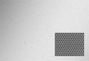
High-Resolution TEM Images
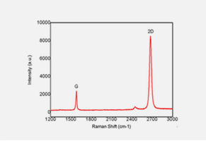
Raman Spectrum (after transfer)
High-Resolution TEM Images
Substrate specifications
| Orientation | <100> |
| Thickness | 525±25 μm |
| Oxide Thickness | 300nm |
| Type/Dopant | P/Boron |
| Resistivity | Resistivity |
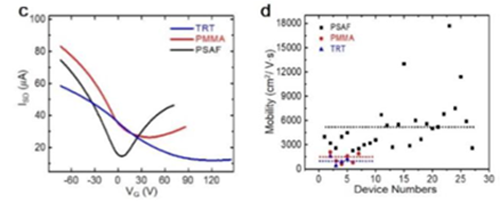
Electrical Properties
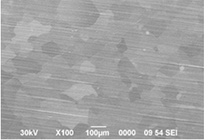
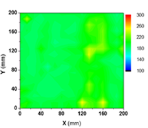
Sheet Resistance Uniformity
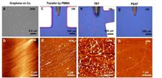
Ultra-Clean Transfer by Pressure Sensitive Adhesive Films
Reference
(1) S. Kim et. al. Ultra-Clean Patterned Transfer of Single-Layer Graphene by Recyclable Pressure Sensitive Adhesive Films. Nano Lett (accepted).
(2) S. Bae*, H. Kim* et al. Roll-to-roll production of 30 inch graphene films for transparent electrodes Nature Nanotech. 5, 574 (2010).


