GRAPHENE SQUARE

Sample

We aspire to provide the best quality products

Graphene on SiO2/Si wafer

Graphene on SiO2/Si wafer

pdf
  • Properties

  • Product Size

    Up to 90x90mm2(Max)

  • Film morphology

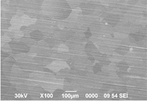
    Continuous Monolayer(>95%)

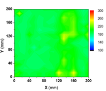
  • Sheet Resistance

    Av. < 250~400 Ω/sq

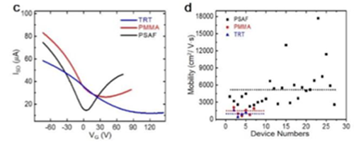
  • Mobility

    >3500cm2/Vs (Max.17,000cm2/Vs

  • Transmittance

    >97%

  • Subtrate

    SiO2 (300mm)/Si wafer (Stard)

  • Domain Size

    10-20 μm

ContactContact

Contact

close button
  • Please complete below information and we will respond as soon as possible :


    1. Country

  • 2. Name of organization

  • 3. Contact person

  • 4. Title

  • 5. E-mail address

Message

Send
EstimatesEstimates

Estimates

close button
  • Please fill in the information below , we'll send you an invoice in the mail within a day.

    1.

  • 2.

  • 3. Name

  • 4. E-mail

Send
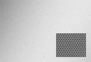
  • High-Resolution TEM Images

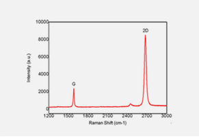
  • Raman Spectrum (after transfer)

  • High-Resolution TEM Images

Substrate specifications

Orientation <100>
Thickness 525±25 μm
Oxide Thickness 300nm
Type/Dopant P/Boron
Resistivity Resistivity
  • Electrical Properties

  • Sheet Resistance Uniformity

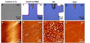
  • Ultra-Clean Transfer by Pressure Sensitive Adhesive Films
Reference

(1) S. Kim et. al. Ultra-Clean Patterned Transfer of Single-Layer Graphene by Recyclable Pressure Sensitive Adhesive Films. Nano Lett (accepted).
(2) S. Bae*, H. Kim* et al. Roll-to-roll production of 30 inch graphene films for transparent electrodes Nature Nanotech. 5, 574 (2010).

5